
Lateral Confinement in 2D Semiconductors
-
Understanding and controlling the optical and electronic behavior of materials can dramatically enhance device functionality for sensing, display, communication, and computation. Low-dimensional materials exhibit novel physical behavior that emerges at small length scales while offering the ability to control material properties by altering their size. In sufficiently small structures like quantum dots (QDs), single electronic states can be spectrally isolated by the confinement-induced energy splitting, which can be harnessed for quantum functionality like single photon emitters and detectors or quantum information processing. Understanding the dynamics of emergent phenomena in low-dimensional systems can enable exploitation of these features in technologies.
-
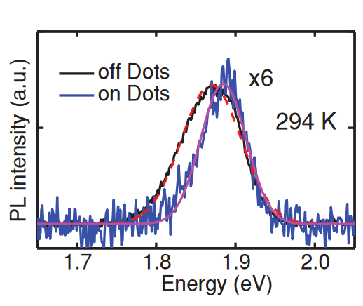
This outlook is exemplified by a new class of two-dimensional (2D) semiconductors called transition metal dichalcogenides (TMDs) in which electronic states are vertically confined by the layered crystal structure. The optical properties of these 2D materials can be tuned by lateral confinement of the electronic states. Although reaching the single electron limit is a challenge in TMD QDs, monolayer TMDs are particularly promising materials for studying spin-orbit phenomena in reduced dimensionality. The inversion asymmetry and spin-orbit coupling in these materials results in a valley index in the band structure that imparts a new property to excitations1. The combination of strong vertical confinement and tunable lateral confinement allows the size of a monolayer nanostructure to couple to this valley pseudospin.2
-
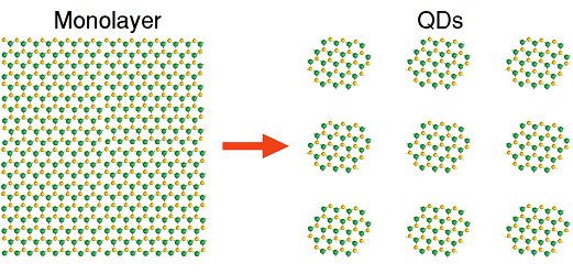
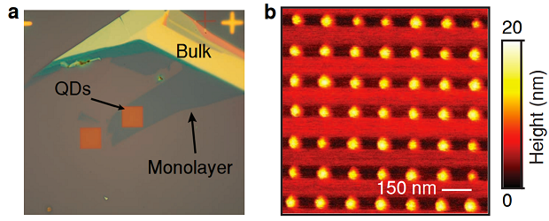
In the Stern Group, we are working to create size-tunable monolayer nanostructures using semiconductor-compatible fabrication techniques with length scales of 10 nm. These structures enable exploration of the relationship between nanostructure size and the dynamics of the valley index using polarization-sensitive optical methods2. To do this, we fabricate QDs on the same size scale as the Bohr radius of excitons in TMDs, which is about 1 nm. Creating such extremely small structures requires the use of novel fabrication techniques, which we are developing in our group. Methods involve ultrahigh-resolution electron-beam lithography and nanoparticle etch masks are used to create atomically-thin materials with lateral dimensions of nanometer scale in rationally designed patterns.
- D. Xiao, G. Liu, W. Feng, X. Xu, and W. Yao.
“Coupled Spin and Valley Physics in Monolayers of MoS2 and Other Group-VI Dichalcogenides.”
PRL, 108, 196802, (2012)
- G. Liu, H. Pang, Y. Yao, and W. Yao
“Intervalley coupling by quantum dot confinement potentials in monolayer transition metal dichalcogenides”
New J. Phys., 16, 105011, (2014)
- G. Wei, D. A. Czaplewski, E. J. Lenferink, T. K. Stanev, I. W. Jung, N. P. Stern
“Valley Polarization in Size-Tunable Monolayer Semiconductor Quantum Dots.”
arXiv:1510.09135, (2015)