
Layer-Dependent Control of Electronic Properties of Two-Dimensional Semiconductors and Heterostructures
-
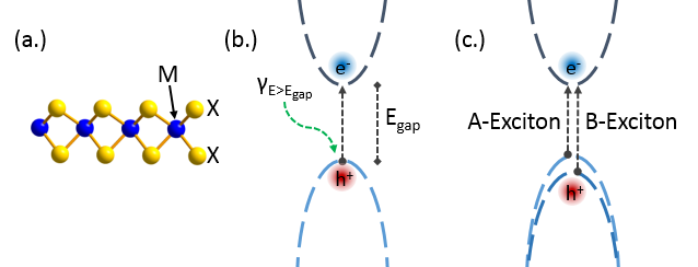
The transition metal dichalcogenides (TMDs) are semiconductor materials with a layered crystal structure consisting of distinct sheets of atoms bonded by van der Waals forces. One of these atomically-thin layers is illustrated in Fig. 1. In many of these materials such as the canonical example of MoS2, the semiconductor band gap depends on the layer number. For example, in its bulk form, MoS2 is an indirect bandgap semiconductor with a transition from the Λ-point in the conduction band to the Γ-point in the valence band. By thinning the material down to two layers, a bilayer, the indirect transition blue shifts from approximately 1.4 eV in bulk to 1.55 eV in the bilayer case and the transition is from the conduction band K-point. Once reduced to a monolayer form, MoS2 becomes a direct bandgap semiconductor with excitonic transitions at the K-points. Large spin-splitting of the valence band leads to large energy separation of the A and B excitons with optical transition energies of 1.9 eV and 2.1 eV, respectively. The quantum efficiency of exciton emission is also layer dependent with a decrease in layer number leading to an increase in emission quantum yield, with the monolayer quantum yield many times greater than that of a bulk stack of MoS2.
-
The layer-dependent electron energies of TMD semiconductors allow band engineering with atomically-thin sheets. By combining monolayers of different TMD materials or layers, vertical or lateral heterostructures can be formed that display novel optical and electronic properties at the interface due to the distinct energetics of each region such as indirect excitons or band bending. Layer-dependent band engineering can be harnessed to rationally design the electronic properties at the interface of a heterostructure. For example, by varying the bandgap with layer number, one-dimensional regions of charge can be confined in analogy with two-dimensional electron gases in bulk semiconductor heterostructures.
-
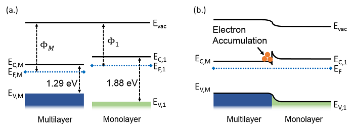
In the Stern Group, we study such low-dimensional electronic regions by isolating interfaces between flakes of MoS2 with different layer number. These naturally occurring homojunction interfaces have less strain and fewer defects than fabricated heterostructures. Because the work functions and band energies differ across the boundary, these devices can support interfacial charge accumulation in the band bending region (Fig. 2).
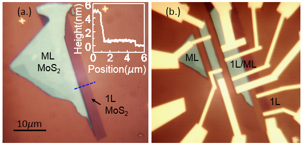
In our recent work1, such exfoliated flakes were patterned to make a monolayer/multilayer heterojunction of MoS2 were obtained by exfoliation and patterned into longitudinal electronic devices (Fig. 3). Band bending is confirmed by luminescence and photocurrent. We observe modification of the effective conductivity of the devices with an enhancement over the monolayer or multilayer properties. This suggests that the electronic state at the interface has modified transport properties. In light of recent measurements of electronic accumulation at layer boundaries2, the one-dimensional interfacial charge state is an interesting system for exploring control of spin and charge transport in layered materials.
- Y. Jia, T. K. Stanev, E. J. Lenferink, and N. P. Stern.
“Enhanced Conductivity Along Lateral Homojunction Interfaces of Atomically Thin Semiconductors.”
Accepted, in press, arXiv:1612.03921, (2017)
- D. Wu, X. Li, L. Luan, X. Wu, W. Li, M. N. Yogeesh, R. Ghosh, Z. Chu, D. Akinwande, Q. Niu, and K. Lai.
“Uncovering edge states and electrical inhomogeneity in MoS2 field-effect transistors.”
Proc. Nat. Acad. Sci., 113, (2016)